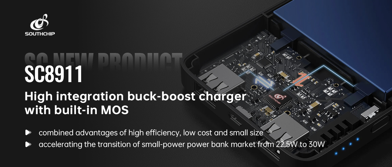
Southchip announced the launch of the fully integrated synchronous bidirectional buck-boost charging chip SC8911. Equipped with an I2C interface, this chip is optimized for common 2-cell, 30W power bank applications in terms of efficiency. It can effectively reduce the case temperature rise, providing users with a safer and more efficient charging experience. SC8911 supports OTG reverse boost functionality and is compatible with multiple modes, including trickle charging, pre-charging, constant current charging, constant voltage charging, and automatic termination. This provides a competitive highly solution as the small power mobile power bank market transitions from 22.5W to 30W, helping customers achieve higher efficiency, lower BOM costs, and smaller BOM sizes.
Integrated MOS Solution with Three Major Highlights
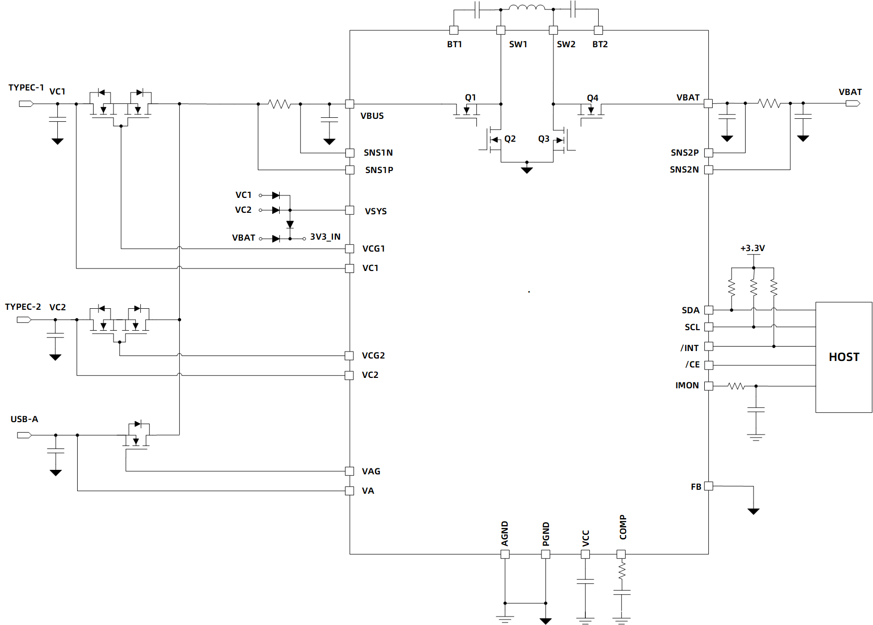
In traditional buck-boost controller solutions with external MOSFETs, PCB traces are often too long due to layout limitations, restricting the driving speed of the power MOSFETs and thus affecting overall efficiency. In contrast, SC8911 features highly integrated design with three NMOS drivers, combining high efficiency, low cost, and small size. In compact applications, SC8911 also offers the following advantages:
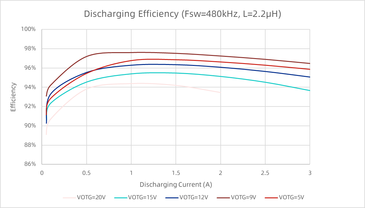
Significantly Improved Efficiency: With built-in power MOSFETs, SC8911 can achieve a switching speed of over 4V/ns, significantly reducing switching losses. Tests show that SC8911 can reach up to 97.6% efficiency. Even under harsh thermal conditions (e.g., battery voltage at 6V, output at 20V/1.5A), the system efficiency remains at 93.5%, with a PCBA temperature of only 69°C, significantly better than the industry average.
More PCB Layout-friendly: The built-in power MOSFETs ensure a small drive loop and power loop path. The package pin design also considers the convenience of placing input and output capacitors. Therefore, SC8911 can easily meet EMI challenges while maintaining high switching speed.
Excellent Thermal Performance: SC8911 uses a 4mm×5mm QFN-27 flip-chip package. The heat generated by the power loss inside the IC can be directly conducted to the PCB through the package copper pillars, effectively enhancing the chip's thermal dissipation capability.
Adapting to Diverse Needs and Simplifying Charging Design
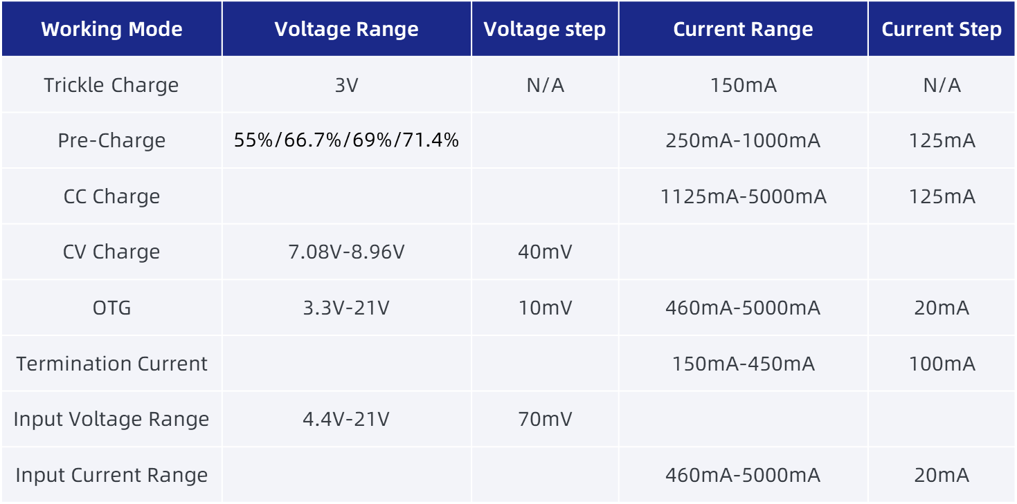
SC8911 features a wide input voltage range of 4.4V to 21V. In standby mode, the static current is as low as 50μA, and in transportation mode, it is as low as 5μA, optimizing the device's power consumption. In terms of charging performance, SC8911 can select three different switching frequencies (240kHz, 360kHz, and 480kHz) via the I2C interface and achieve current and voltage regulation throughout the entire charging cycle. The charging voltage control accuracy can reach up to ±0.5%. For the reverse OTG function, SC8911 supports fine voltage step regulation of 10mV, meeting the requirements of PD and UFCS protocols and supporting diverse needs of end devices.
.png)
The integration of SC8911 also brings great convenience to the charging design:
SC8911 provides integrated port low-current detection and load detection functions, eliminating the need for port current detection resistors and A-port load detection circuits in the system.
By optimizing system logic, SC8911 reduces I/O port requirements and lowers the threshold for protocol chips during use.
Using SC8911 allows the system to eliminate port discharge and adapter insertion detection circuits, and replace the port isolation P-channel MOSFET with an N-channel MOSFET, further reducing BOM size and cost.
.png)
Multiple Detection and Protection Mechanisms to Safeguard the Charging Process
SC8911 offers various detection functions, precisely measuring parameters such as input current, input voltage, battery current, battery voltage, junction temperature, and output current, ensuring full control over the entire charging process. Based on this, SC8911 integrates multiple protection mechanisms, including overvoltage protection for ports and batteries, output overvoltage protection, short-circuit protection, cycle-by-cycle current limiting, and thermal shutdown protection, effectively ensuring the safety and stability of the charging process.